

Master how to simulate JFET circuit on Proteus with our step-by-step guide. Optimize your learning journey today! Read more.
Meet Swarit Mahalsekar, the Biomedical engineer who has made it his mission to share his knowledge and skills in electronics with the world. As an experienced online instructor on multiple platforms, Swarit has helped countless students master the art of electronics. But that's not all – Swarit's passion for teaching led him to found "Practical Buddy," a platform dedicated to providing students with practical, hands-on experience in electronics. With his extensive background in completing e
Access all courses in our library for only $9/month with All Access Pass
Get Started with All Access PassBuy Only This CourseAbout This Course
Who this course is for:
- Students who want to learn FETs
- Students who want to understand transistors in depth
- Students who want to learn analog electronics in depth
- Students who to learn analog circuit design
- Advanced JFET Analysis and Design with Proteus
- Analog Electronics and circuits with JFET on Proteus
- Proteus Simulation for JFET Biasing and Amplifier Design
What you’ll learn:
- Understand the basic principle of FET’s
- Fundamentals of JFET Circuit Design and Simulation
- Learn the type and symbol of JFET
- Construction or Internal structure of JFET
- How to operate JFET as a switch
- How to operate JFET as an amplifier
- Proteus circuit simulator
- Configurations of JFETs (CG, CD, CS)
- JFET Amplifiers and Switching Circuits on Proteus
- Characteristics of JFETs (Transfer Characteristic and Drain Source Characteristics)
- Biasing of JFET
- Small signal analysis of JFET or JFET as an Amplifier
- Advanced JFET Analysis and Design with Proteus
Requirements:
- Basic knowledge of current electricity or you can learn it through my course Current Electricity In Depth And Basics Of DC Circuits and learn all those concepts.
- In depth knowledge of Semiconductors. If you don’t know these concepts, you can enroll in my course Semiconductors And Its Application In Analog Electronics.
- In depth knowledge about working of diodes and diode circuits. If you don’t know these concepts, enroll in my course Analog Electronics For Beginners – Simulating Circuits On Electric Circuit Studio.
- In depth knowledge of BJTs or you can learn it through my course Analog Electronics Part 2: Understand, Design And Simulate Transistors Based Circuits On Proteus Software
- Circuit simulation on Tinkercad and Proteus software
Do you know what FETs (Field Effect Transistors) are, the principles and workings of FETs, etc? Don’t worry even if you don’t know anything about FETs. In this course, we are going to see JFETs (Junction Field Effect Transistors) which are very easy to understand as compared to MOSFETs (Metal Oxide Silicon Field Effect Transistors).
Our Promise to You
By the end of this course, you will have learned all about how to simulate JFET Circuit On Proteus.
10 Day Money Back Guarantee. If you are unsatisfied for any reason, simply contact us and we’ll give you a full refund. No questions asked.
Explore and how to simulate JFET circuit on Proteus now! Dive into hands-on learning for a tech-savvy journey.
Course Curriculum
| Section 1 - Introduction | |||
| Introduction | 00:00:00 | ||
| Type And Symbol Of JFET | 00:00:00 | ||
| Construction Or Internal Structure Of JFET | 00:00:00 | ||
| Section 2 - Working Of JFET | |||
| Why Depletion Region Is Wider At The Top And Narrower At The Bottom? | 00:00:00 | ||
| Why N-Channel JFET Is Preferred Over P-Channel JFET? | 00:00:00 | ||
| Understand The Working Of N-Channel-JFET | 00:00:00 | ||
| Section 3 - Characteristics Of JFET | |||
| Why The Internal Input Impedance Of An Amplifier Should Be As High As Possible? | 00:00:00 | ||
| Configurations Of JFET | 00:00:00 | ||
| Transfer Characteristics Of JFET | 00:00:00 | ||
| Expansion Of Depletion Region | 00:00:00 | ||
| Drain Source Characteristics | 00:00:00 | ||
| Understanding Pinch-Off Condition | 00:00:00 | ||
| Section 4 - Operating Regions Of JFET | |||
| Cutoff Region | 00:00:00 | ||
| Saturation Region | 00:00:00 | ||
| Ohmic Region | 00:00:00 | ||
| Section 5 - Understanding The Data-Sheet Of BFW10 And Drain Current Equation Of JFET | |||
| Drain Current Equation Of JFET | 00:00:00 | ||
| Understanding The Data-Sheet Of BFW10 | 00:00:00 | ||
| Mistake In Few Datasheet Of BFW10 And BFW11 | 00:00:00 | ||
| Section 6 - Identify Terminals Of JFET | |||
| Shortcut Trick To Identify The Terminals Of JFET | 00:00:00 | ||
| Identify Terminals Of BFW0 (Practically) | 00:00:00 | ||
| Section 7 - Understanding The Conditions To Operate BFW10 In Cutoff And Saturation Region | |||
| Operating JFET In Cutoff And Saturation Region | 00:00:00 | ||
| Simulating JFET As A Switch In Multisim Software | 00:00:00 | ||
| Section 8 - Important Parameters Of JFET | |||
| Dynamic Drain Resistance | 00:00:00 | ||
| Transconductance Formula With It's Derivation | 00:00:00 | ||
| Amplification Factor | 00:00:00 | ||
| Section 9 - Zero Temperature Drift Concept | |||
| Zero Temperature Drift (Part 1) | 00:00:00 | ||
| Zero Temperature Drift (Part 2) | 00:00:00 | ||
| Section 10 - Biasing Techniques In JFET | |||
| Understanding The Significance Of Q-Point And Biasing The JFET | 00:00:00 | ||
| Fixed Bias Technique Of JFET | 00:00:00 | ||
| Self Bias Technique Of JFET | 00:00:00 | ||
| Voltage Divider Bias Technique Of JFET | 00:00:00 | ||
| Section 11 - Variation Of Pinch-Off Voltage (Vp = Vgsoff) | |||
| What Is Maximum, Minimum And Typical Value Of Vp And Which Value We Should Consider? | 00:00:00 | ||
| Section 12 - Numericals On JFET | |||
| Numerical 1 | 00:00:00 | ||
| Simulation Of Numerical 1 | 00:00:00 | ||
| Numerical 2 | 00:00:00 | ||
| Section 13 - AC Modelling Of JFET | |||
| Modelling Of JFET (Part 1) | 00:00:00 | ||
| Modelling Of JFET (Part 2) | 00:00:00 | ||
| Section 14 - Analyzing Common Source And Common Gate Amplifier | |||
| CS Amplifier (Without CS Capacitor) | 00:00:00 | ||
| CS Amplifier (With CS Capacitor) | 00:00:00 | ||
| CG Amplifier (Common Gate Amplifier) | 00:00:00 | ||
| Why We Prefer Common Source Over Common Gate Amplifier | 00:00:00 | ||
| Section 15 - JFETs Vs BJTs Complete Analysis | |||
| JFETs Vs BJTs | 00:00:00 | ||
| Section 16 - Designing And Simulating Cs Amplifier On Proteus And Multisim | |||
| Designing JFET Based CS Amplifier | 00:00:00 | ||
| Simulation Of CS Amplifier On Proteus And On Multisim | 00:00:00 | ||
About This Course
Who this course is for:
- Students who want to learn FETs
- Students who want to understand transistors in depth
- Students who want to learn analog electronics in depth
- Students who to learn analog circuit design
- Advanced JFET Analysis and Design with Proteus
- Analog Electronics and circuits with JFET on Proteus
- Proteus Simulation for JFET Biasing and Amplifier Design
What you’ll learn:
- Understand the basic principle of FET’s
- Fundamentals of JFET Circuit Design and Simulation
- Learn the type and symbol of JFET
- Construction or Internal structure of JFET
- How to operate JFET as a switch
- How to operate JFET as an amplifier
- Proteus circuit simulator
- Configurations of JFETs (CG, CD, CS)
- JFET Amplifiers and Switching Circuits on Proteus
- Characteristics of JFETs (Transfer Characteristic and Drain Source Characteristics)
- Biasing of JFET
- Small signal analysis of JFET or JFET as an Amplifier
- Advanced JFET Analysis and Design with Proteus
Requirements:
- Basic knowledge of current electricity or you can learn it through my course Current Electricity In Depth And Basics Of DC Circuits and learn all those concepts.
- In depth knowledge of Semiconductors. If you don’t know these concepts, you can enroll in my course Semiconductors And Its Application In Analog Electronics.
- In depth knowledge about working of diodes and diode circuits. If you don’t know these concepts, enroll in my course Analog Electronics For Beginners – Simulating Circuits On Electric Circuit Studio.
- In depth knowledge of BJTs or you can learn it through my course Analog Electronics Part 2: Understand, Design And Simulate Transistors Based Circuits On Proteus Software
- Circuit simulation on Tinkercad and Proteus software
Do you know what FETs (Field Effect Transistors) are, the principles and workings of FETs, etc? Don’t worry even if you don’t know anything about FETs. In this course, we are going to see JFETs (Junction Field Effect Transistors) which are very easy to understand as compared to MOSFETs (Metal Oxide Silicon Field Effect Transistors).
Our Promise to You
By the end of this course, you will have learned all about how to simulate JFET Circuit On Proteus.
10 Day Money Back Guarantee. If you are unsatisfied for any reason, simply contact us and we’ll give you a full refund. No questions asked.
Explore and how to simulate JFET circuit on Proteus now! Dive into hands-on learning for a tech-savvy journey.
Course Curriculum
| Section 1 - Introduction | |||
| Introduction | 00:00:00 | ||
| Type And Symbol Of JFET | 00:00:00 | ||
| Construction Or Internal Structure Of JFET | 00:00:00 | ||
| Section 2 - Working Of JFET | |||
| Why Depletion Region Is Wider At The Top And Narrower At The Bottom? | 00:00:00 | ||
| Why N-Channel JFET Is Preferred Over P-Channel JFET? | 00:00:00 | ||
| Understand The Working Of N-Channel-JFET | 00:00:00 | ||
| Section 3 - Characteristics Of JFET | |||
| Why The Internal Input Impedance Of An Amplifier Should Be As High As Possible? | 00:00:00 | ||
| Configurations Of JFET | 00:00:00 | ||
| Transfer Characteristics Of JFET | 00:00:00 | ||
| Expansion Of Depletion Region | 00:00:00 | ||
| Drain Source Characteristics | 00:00:00 | ||
| Understanding Pinch-Off Condition | 00:00:00 | ||
| Section 4 - Operating Regions Of JFET | |||
| Cutoff Region | 00:00:00 | ||
| Saturation Region | 00:00:00 | ||
| Ohmic Region | 00:00:00 | ||
| Section 5 - Understanding The Data-Sheet Of BFW10 And Drain Current Equation Of JFET | |||
| Drain Current Equation Of JFET | 00:00:00 | ||
| Understanding The Data-Sheet Of BFW10 | 00:00:00 | ||
| Mistake In Few Datasheet Of BFW10 And BFW11 | 00:00:00 | ||
| Section 6 - Identify Terminals Of JFET | |||
| Shortcut Trick To Identify The Terminals Of JFET | 00:00:00 | ||
| Identify Terminals Of BFW0 (Practically) | 00:00:00 | ||
| Section 7 - Understanding The Conditions To Operate BFW10 In Cutoff And Saturation Region | |||
| Operating JFET In Cutoff And Saturation Region | 00:00:00 | ||
| Simulating JFET As A Switch In Multisim Software | 00:00:00 | ||
| Section 8 - Important Parameters Of JFET | |||
| Dynamic Drain Resistance | 00:00:00 | ||
| Transconductance Formula With It's Derivation | 00:00:00 | ||
| Amplification Factor | 00:00:00 | ||
| Section 9 - Zero Temperature Drift Concept | |||
| Zero Temperature Drift (Part 1) | 00:00:00 | ||
| Zero Temperature Drift (Part 2) | 00:00:00 | ||
| Section 10 - Biasing Techniques In JFET | |||
| Understanding The Significance Of Q-Point And Biasing The JFET | 00:00:00 | ||
| Fixed Bias Technique Of JFET | 00:00:00 | ||
| Self Bias Technique Of JFET | 00:00:00 | ||
| Voltage Divider Bias Technique Of JFET | 00:00:00 | ||
| Section 11 - Variation Of Pinch-Off Voltage (Vp = Vgsoff) | |||
| What Is Maximum, Minimum And Typical Value Of Vp And Which Value We Should Consider? | 00:00:00 | ||
| Section 12 - Numericals On JFET | |||
| Numerical 1 | 00:00:00 | ||
| Simulation Of Numerical 1 | 00:00:00 | ||
| Numerical 2 | 00:00:00 | ||
| Section 13 - AC Modelling Of JFET | |||
| Modelling Of JFET (Part 1) | 00:00:00 | ||
| Modelling Of JFET (Part 2) | 00:00:00 | ||
| Section 14 - Analyzing Common Source And Common Gate Amplifier | |||
| CS Amplifier (Without CS Capacitor) | 00:00:00 | ||
| CS Amplifier (With CS Capacitor) | 00:00:00 | ||
| CG Amplifier (Common Gate Amplifier) | 00:00:00 | ||
| Why We Prefer Common Source Over Common Gate Amplifier | 00:00:00 | ||
| Section 15 - JFETs Vs BJTs Complete Analysis | |||
| JFETs Vs BJTs | 00:00:00 | ||
| Section 16 - Designing And Simulating Cs Amplifier On Proteus And Multisim | |||
| Designing JFET Based CS Amplifier | 00:00:00 | ||
| Simulation Of CS Amplifier On Proteus And On Multisim | 00:00:00 | ||
Related Courses

Analog Electronics For Beginners - Simulating Circuits On Electric Circuit Studio
BeginnerSwarit Mahalsekar$199.00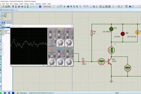
Analog Electronics Part 2: Understand, Design And Simulate Transistors Based Circuits On Proteus Software
IntermediateSwarit Mahalsekar$199.00

Analog Electronics For Beginners - Simulating Circuits On Electric Circuit Studio

Analog Electronics Part 2: Understand, Design And Simulate Transistors Based Circuits On Proteus Software

Are you interested in higher education?
All Rights Reserved